芯片电磁仿真解决方案
EM Simulation for ICs
介绍
Introduction
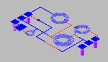
法动科技芯片级的电磁仿真软件UltraEM®采用领先的三维全波电磁仿真技术,用于分析射频/微波IC及高速数字IC版图的电磁场效应,并与业界领先的模拟芯片设计环境进行无缝集成,为广大的设计人员提供高精度电磁分析服务。本案例展示5G带通滤波器芯片的仿真流程,该滤波器工作频率3.3GHz-4.2GHz,中心频率为3.8GHz,通带最大衰减为-2dB。
UltraEM®, the 3D Full-wave EM Simulation software from Faraday Dynamics, Ltd., is designed to analyze the electromagnetic field effects of RF/microwave IC and high-speed digital IC layouts. It can be seamlessly integrated with the industry's leading analog chip design environments to provide high-precision electromagnetic analysis services for designers. This reference case demonstrates the simulation task of a 5G bandpass filter design using a gallium arsenide process, that operates at a frequency range from 3.3GHz to 4.2GHz, a center frequency of 3.8GHz, and a maximum passband attenuation of -2dB.
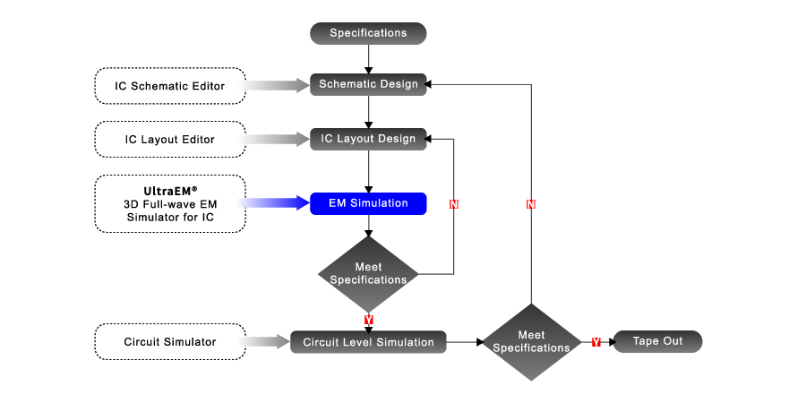
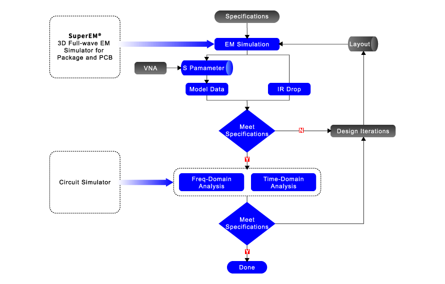
设计流程
Design Flow
仿真结果
Simulation Results
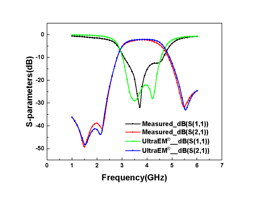
仿真结果与实测数据对比显示,该带通滤波器在3.3-4.2GHz的工作频段内的衰减不大于-2dB,端口之间的耦合小于-10dB,且频偏小于0.1GHz。
The simulation results and the measured results are compared in the above figure. It shows that the attenuation of the filter within the operating frequency band of 3.3-4.2GHz is not more than -2dB, the coupling between ports is less than -10dB, and the frequency offset is less than 0.1GHz.
EDA软件
EDA Tools


介绍
Introduction
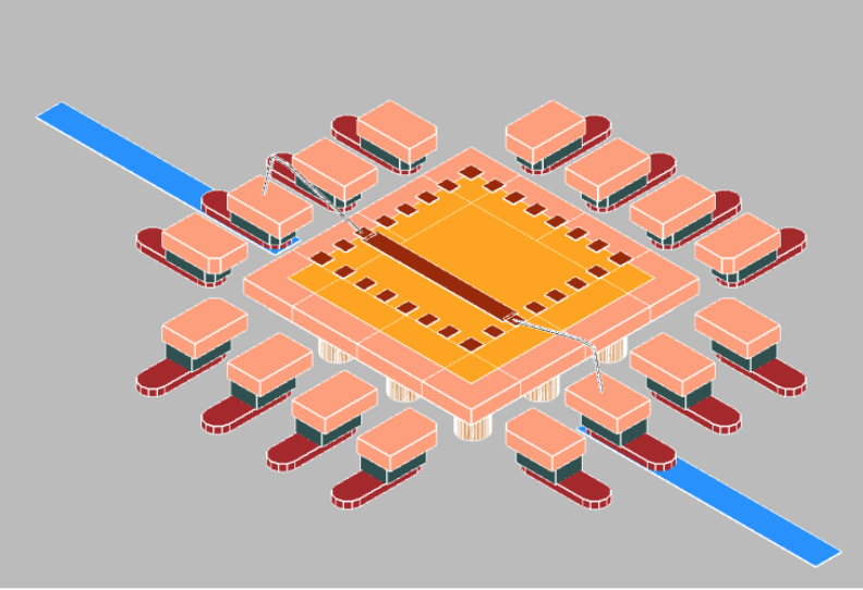
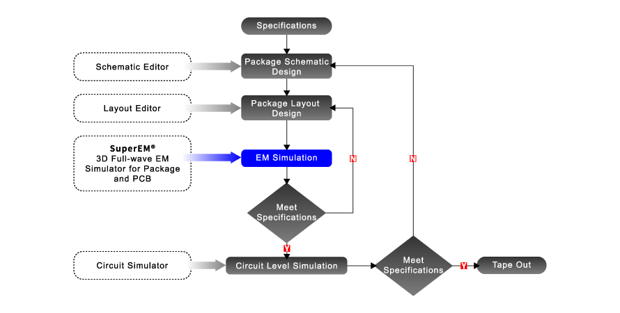
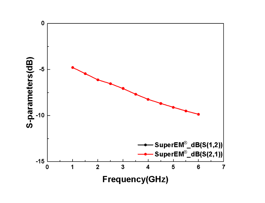
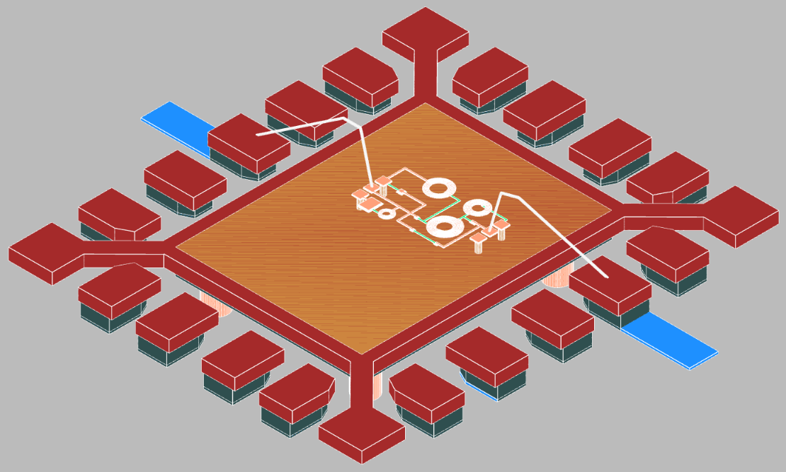
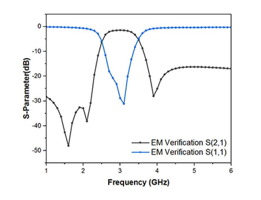
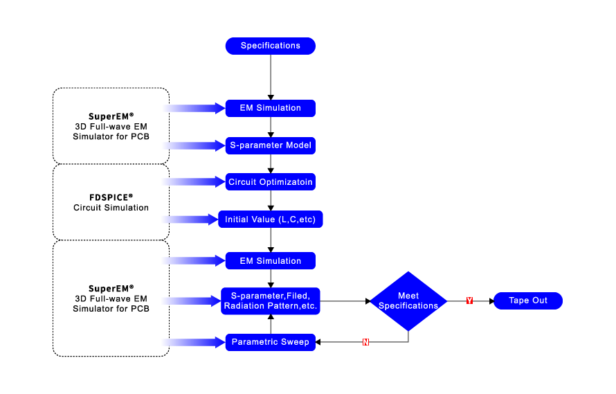
法动科技针对封装和PCB级的电磁仿真软件SuperEM®采用领先的三维全波电磁仿真技术,用于分析高速PCB和IC封装的电磁场效应,并与业界领先的模拟芯片设计环境进行无缝整合,为广大的设计人员提供高精度电磁分析服务,以黄金标准精度应对更复杂的电磁(EM)挑战,本案例将展示QFN(方形扁平无引脚封装)的S参数仿真流程以供参考。
The simulation results and the measured results are compared in the above figure. It shows that the attenuation of the filter within the operating frequency band of 3.3-4.2GHz is not more than -2dB, the coupling between ports is less than -10dB, and the frequency offset is less than 0.1GHz. SuperEM®, the package and PCB EM simulation software from Faraday Dynamics, Ltd. adopts the most advanced 3D full-wave EM simulation technology for analyzing the electromagnetic field effects of high-speed IC packages and PCBs. It can be seamlessly integrated with the industry's leading package and PCB design environments to provide high precision EM analysis services to attack very complex EM challenges with gold-standard precision. This reference case demonstrates the SuperEM® S-parameter simulation task of a Quad Flat No-leads (QFN) design.
设计流程
Design Flow
仿真结果
Simulation Results
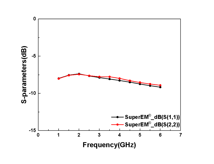
本案例介绍了采用法动科技的SuperEM®三维全波电磁软件对QFN模型的仿真。SuperEM®易于上手的界面实现了工艺配置、模型导入、端口创建等功能,快速完成模型的建模和仿真,可满足用户对封装进行快速建模仿真的应用场景需求。
This example case demonstrates the simulation of a QFN packaging model using SuperEM®. SuperEM® provides a user-friendly interface for process parameters configuration, layout import, port creation, etc. It can satisfy user's needs for rapid modeling and simulation of packaging design scenarios.
EDA软件
EDA Tools


介绍
Introduction
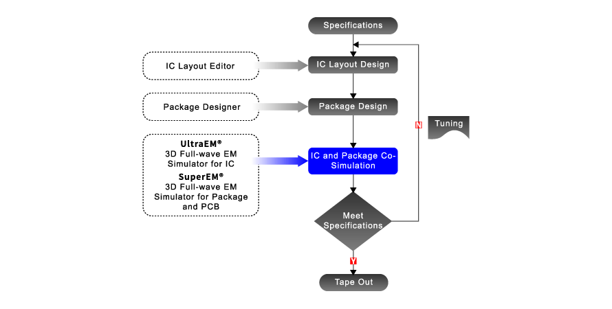
芯片设计与封装设计传统上是由各自工程团队独立完成,这样做的缺陷是增加了迭代时间和沟通成本。法动科技独创芯片-封装联合仿真流程,三维建模简单易用,并配有专门针对联合仿真的优化求解器,不仅可大幅减少迭代次数,提高设计成功率,而且能使芯片工程师在设计流程中随时评估封装性能。本案例展示5G带通滤波器芯片-封装联合仿真流程,该滤波器工作频率为3.3GHz-4.2GHz,中心频率为3.8GHz。
Traditionally, chip design and package design are developed separately by different engineering teams. It imposes considerable iteration time and high communication costs. Faraday Dynamics® has developed a unique chip and package co-simulation flow. It provides easy-to-use 3D modeling capability and a specially designed simulation solver for co-simulation, which can reduce the number of iterations; improve the design success rate; and enable chip engineers to assess the package performance at any time during the design process. This reference case demonstrates the co-simulation task of a 5G bandpass filter design using a gallium arsenide process that operates at a frequency range from 3.3GHz to 4.2GHz, a center frequency of 3.8GHz.
设计流程
Design Flow
仿真结果
Simulation Results
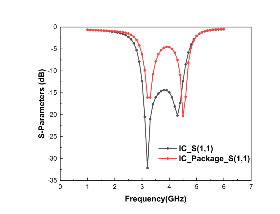
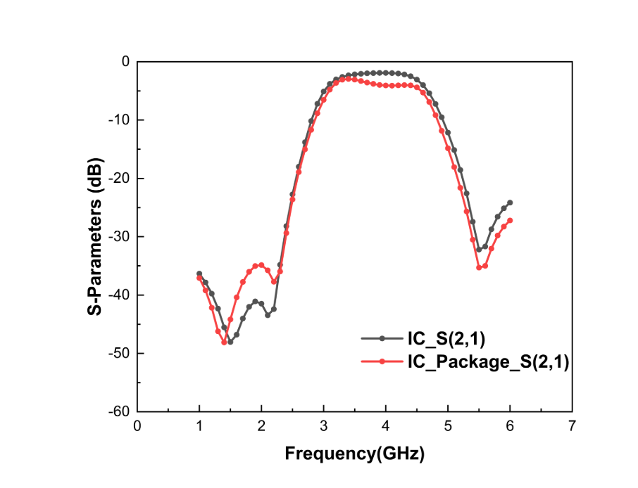
芯片与芯片-封装回波损耗与插入损耗的结果对比
Comparison of Chip-Only vs. Chip-Package Return Loss and Insertion Loss Results
分别仿真了芯片不带封装和带封装两种应用场景,来分析封装对芯片滤波特性的影响。添加封装后滤波器中心频率及通带并没明显变化,通带最大衰减由原来的-2dB变为了-4dB。得出结论: 封装效应是芯片设计不得不考虑的重要因素。我们需要通过封装联合仿真的结果调整芯片版图以达到目标结果。
The chip-only and chip-with-package scenarios are simulated to analyze the effect of the package on the filter. The comparison of results shows that the chip-with-package center frequency and passband characteristics are almost the same as the chip-only case. However, the chip-with package passband maximum attenuation has changed from -2dB to -4dB. With the co-simulation, we can conclude that further chip design refinement must be done to meet the original design target.
EDA软件
EDA Tools
介绍
Introduction
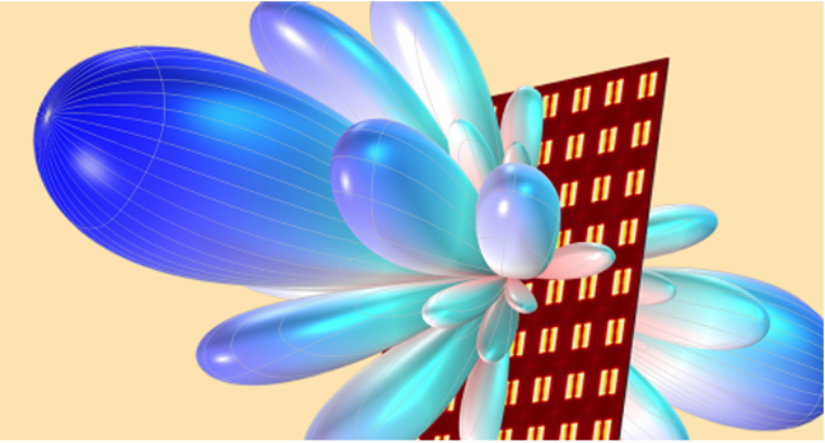
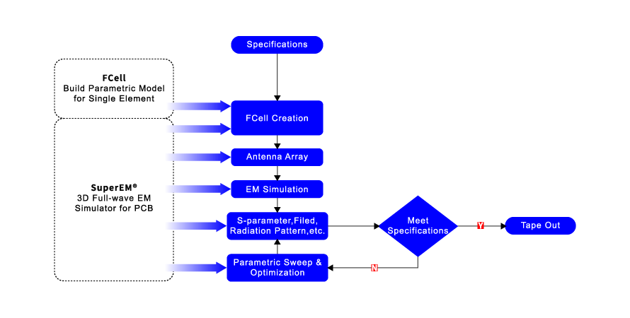
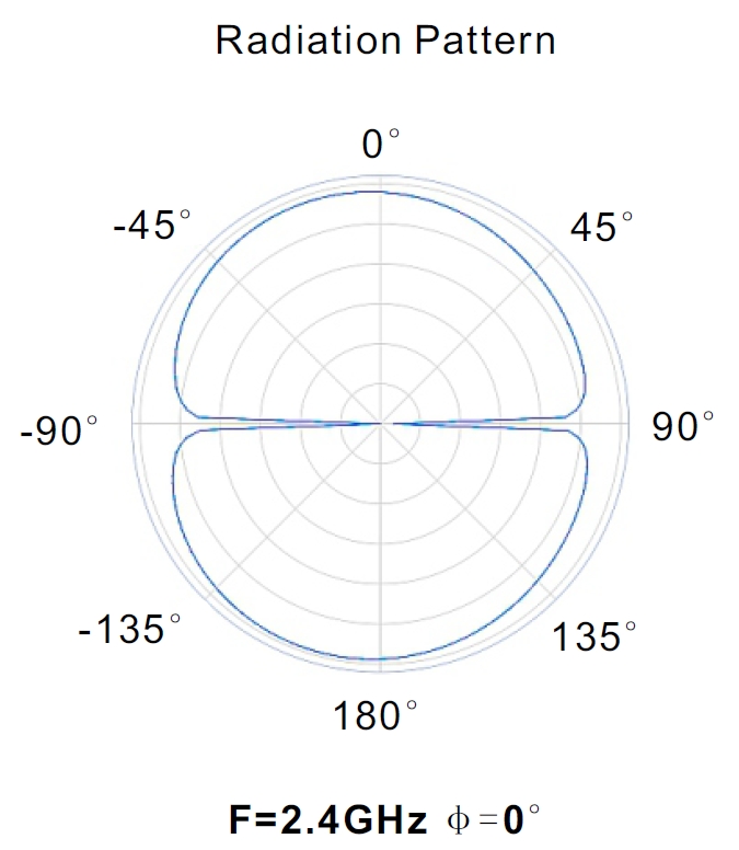
贴片天线拥有小型化、低剖面、高增益、易安装、以及低成本等特点。由贴片天线构成的大规模阵列在毫米波基站、卫星通信、汽车雷达、以及工业物联网等无线通信系统中得到广泛应用。SuperEM®可适用于任何贴片天线阵列的完整设计流程,包括从仿真到调试的各个环节。它可以精确地仿真S参数、近场、以及辐射方向图等数据。本案例展示了一个4×4的贴片天线阵列,单元间隔为半波长,工作频率为3.5GHz,仿真结果数据从SuperEM®导出。
Patch antennas possess merits such as miniaturization, low profile, high gain, easy installation, and low cost. Large-scale arrays composed of patch antennas find extensive applications in wireless communication systems, including millimeter-wave base stations, satellite communications, automotive radar, and industrial IoT. SuperEM® is applicable to the comprehensive design process of any type of patch antenna arrays, covering various stages from simulation to optimization. It accurately simulates data such as S-parameters, near field, and radiation patterns. This case study presents a 4×4 patch antenna array with a unit spacing of half wavelength, operating at 3.5GHz, and the simulation results are exported from SuperEM®.
设计流程
Design Flow
仿真结果
Simulation Results
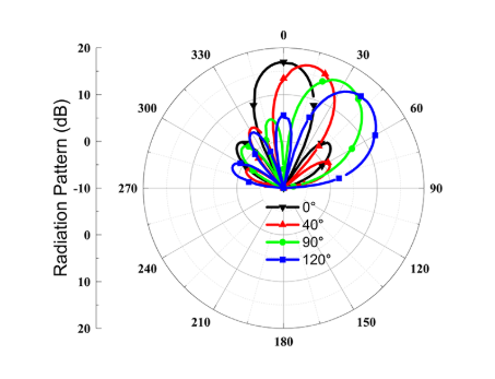
SuperEM®使用FCell模型构建天线单元,只需一次设计,即可用于各种不同板材和尺寸的模型。仿真结果显示,该天线在3.5GHz频段的回波损耗小于10dB,端口之间的耦合小于15dB,且在60度内的扫描增益为14-15dBi,性能优异,适用于大规模波束扫描阵列。
Utilizing the FCell model from one time design, SuperEM® facilitates antenna unit construction, applicable to v arious materials and dimensions. The simulations demonstrate that the antenna array exhibits a return loss of less than 10dB in the 3.5GHz frequency range, coupling between ports is below 15dB, and the scanning gain within 60-degree ranges from 14-15dBi. The performance is exceptional, making it suitable for large scale beam-scanning arrays.
EDA软件
EDA Tools
介绍
Introduction
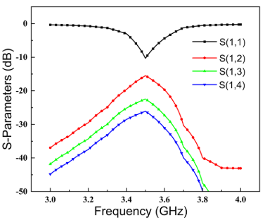
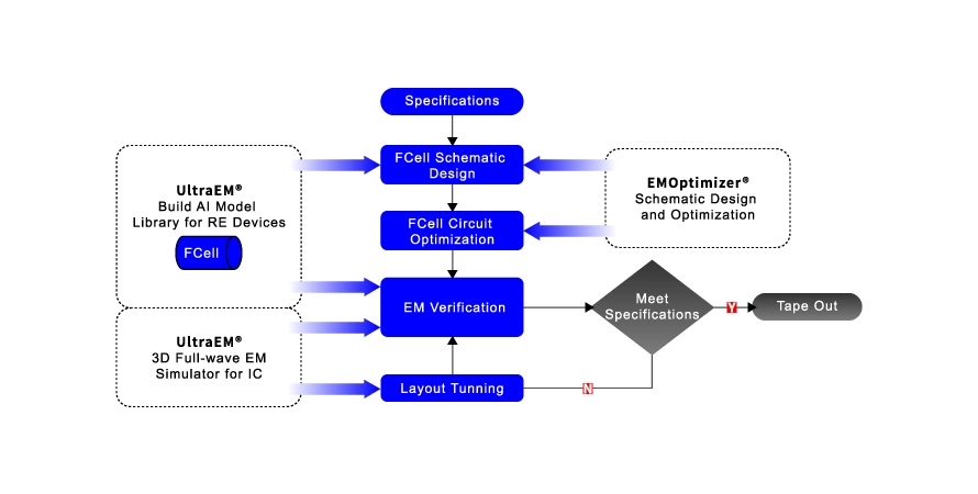
EMOptimizer®是法动科技的射频电路快速设计优化软件。同时EMOptimizer®也是业界首款射频电路快速设计优化软件,该软件将FCell 用于电路设计,在保证较高精度的同时,大大提升电路仿真和优化的速度。本参考案例演示了设计优化一个带通滤波器,通带:2.6GHz-3.2GHz,插入损耗:1.1dB,回波损耗:17dB,衰减:20dB@1.9GHz-2.3GHz,35dB@1.4GHz-1.8GHz,20dB@3.8GHz-4.2GHz,18dB@4.5GHz-6.5GHz。
Powered by the FCell modeling technology, EMOptimizer® (which is industry’s first rapid tool for design and optimization of RF circuits developed by Faraday Dynamics) unleashes unpreceded speed for RF circuit design and optimization, empowering RF design engineers to accomplish their designs much faster than ever before. This reference design case demonstrates design and optimization of a bandpass filter. EMOptimizer® optimizes the filter’s design parameters to achieve a passband of 2.6GHz-3.2GHz with insertion loss (1.1dB) and return loss (17dB). Furthermore, the final filter delivers sharp attenuation in stopbands, 20dB@1.9GHz-2.3GHz, 35dB@1.4GHz-1.8GHz, 20dB@3.8GHz-4.2GHz, and 1.8dB@4.5GHz-6.5GHz.
设计流程
Design Flow
仿真结果
Simulation Results
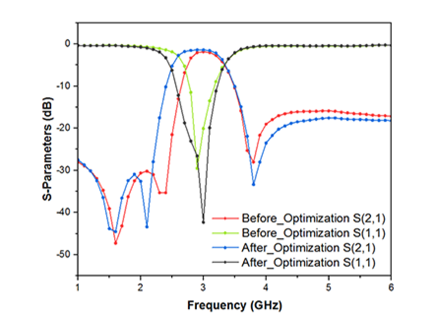
上图是设计的滤波器经过EMOptimizer®优化前后的仿真结果图。经过优化后通带由2.85GHz-3.1GHz增加到2.7GHz-3.1GHz,插入损耗减小0.8dB,回波损耗增加9dB。
The figure depicts the simulation results of the designed filter before and after EMOptimizer® performs optimization. After optimization, the passband increases from 2.85GHz-3.1GHz to 2.7GHz-3.1GHz, the insertion loss is reduced by 0.8 dB, and the return loss increases by 9 dB。
将EMOptimizer®优化得到的版图输出到电磁仿真软件UltraEM®。经电磁仿真验证可见结果达到了设计规格要求。
The optimized layout obtained from EMOptimizer® is exported to UltraEM® for rigorous EM simulation and verification. The EM simulation validates that the final layout design meets the design specifications.
EDA软件
EDA Tools


介绍
Introduction
信号完整性用于评估信号在封装及电路板中的传输和反射情况,以确保信号质量在正常范围内。仿真通常包括时域仿真和频域仿真,前者可用于评估传输线上的波形和反射,后者可用于评估信号的频率响应和带宽。电源完整性仿真是对电源系统的设计进行分析和优化的过程,主要用于评估电源噪声和电源干扰对电路性能的影响,从而优化电源设计。法动科技采用领先的三维全波电磁仿真技术和频域/时域电路仿真算法,可以帮助工程师进行仿真分析,优化封装及电路板设计,并与业界领先的封装及电路板设计环境进行无缝集成,为广大的设计人员提供高精度分析服务。
Signal Integrity (SI) analysis evaluates the transmission and reflection of signals in packages and circuit boards to ensure that the signal quality is within normal limits. SI analysis typically includes time domain simulation, which is used to evaluate waveforms and reflections on transmission lines, and frequency domain simulation, which is used to evaluate the frequency response and bandwidth of signals. Power Integrity (PI) analysis evaluates the impact of power supply noise and power supply interference on circuit performance for power supply design optimization. Faraday Dynamics offers cutting-edge 3D full-wave electromagnetic simulation technology and frequency-/time-domain circuit simulation algorithms for engineers to perform simulation analysis and optimize package and PCB design. They seamlessly integrate with the industry's leading package and board design environments to provide high-precision analysis services to a wide range of designers.
设计流程
Design Flow
仿真结果
Simulation Results
本案例介绍了采用法动科技的SuperEM®对封装及电路板中的信号线仿真电磁特性、提取参数,使用FDSPICE®进行时域仿真的流程。软件界面易于上手,可快速完成建模仿真,可满足用户对设计进行信号完整性分析的需求。
This case describes the flow of simulating electromagnetic characteristics and extracting parameters of signal lines in packages and circuit boards by using SuperEM® from Faraday Dynamics, and the flow of time-domain simulation by using FDSPICE®. The software interface is easy to use and can quickly complete the modeling and simulation, which can meet the user's needs for signal integrity analysis of the design.


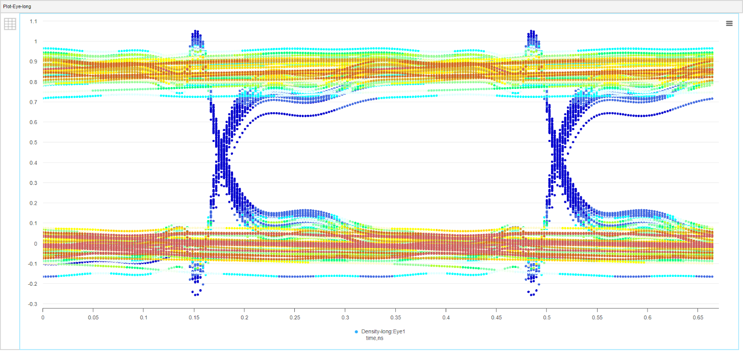
眼图结果
Eye Diagram Result in Inter-code Crosstalk


IR Drop
IR Drop
本案例介绍了采用法动科技SuperEM®对PCB中的电源和地网络仿真IR Drop的流程。软件与业界领先的PCB设计环境进行无缝集成,可以快速读取设计数据,并进行设置仿真,可满足用户进行IR Drop分析的需求。
This case describes the flow of IR Drop simulation of power and ground networks in PCBs using SuperEM®. The software seamlessly integrates with industry-leading PCB design environments to quickly read design data and set up simulations that can meet users' needs for IR Drop analysis.
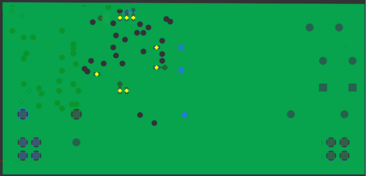
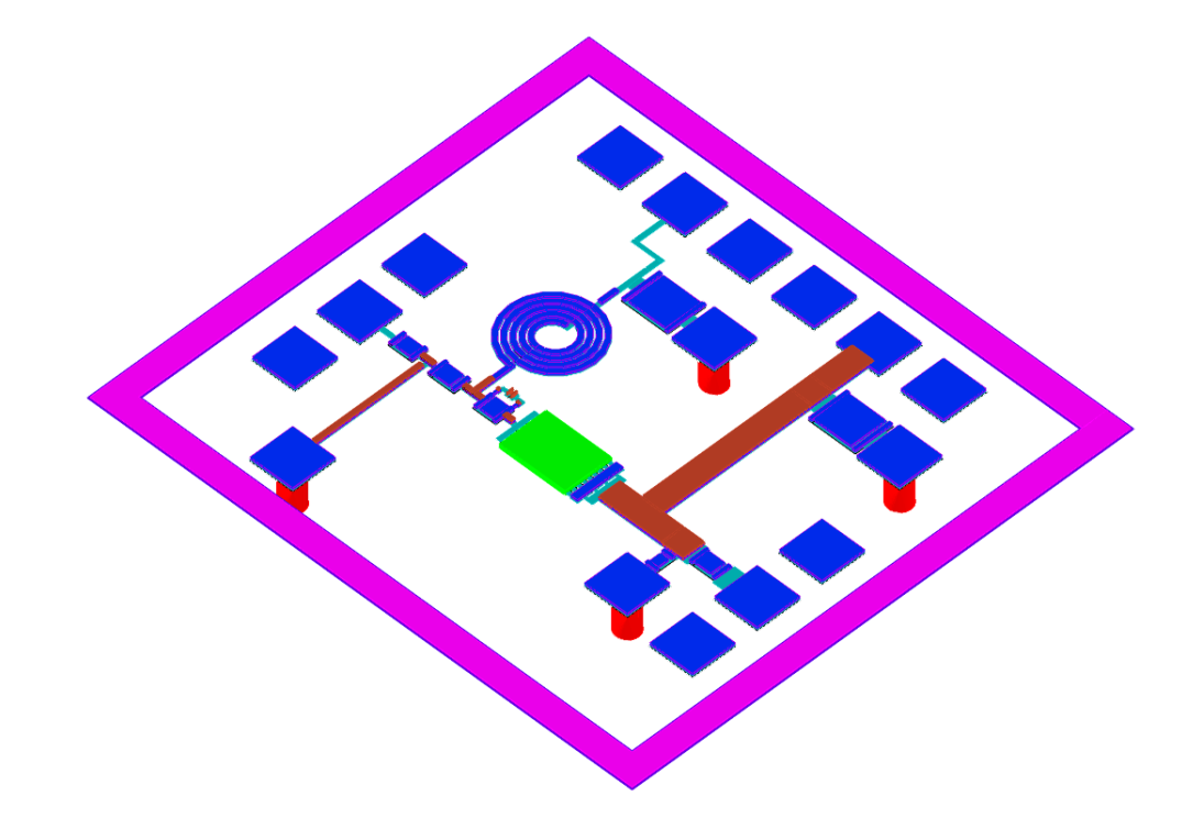
仿真版图
Example for IR Drop
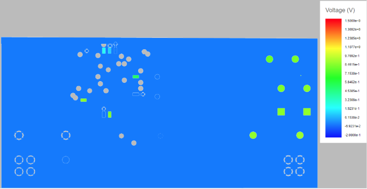
电压分布图
Voltage Distribution Map
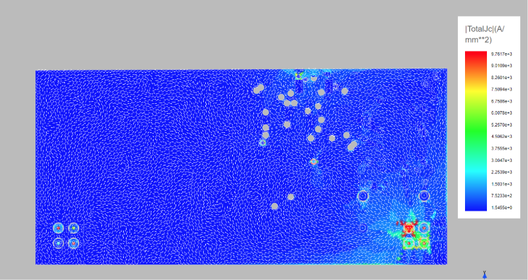
电流密度分布图
Current Density Distribution Map
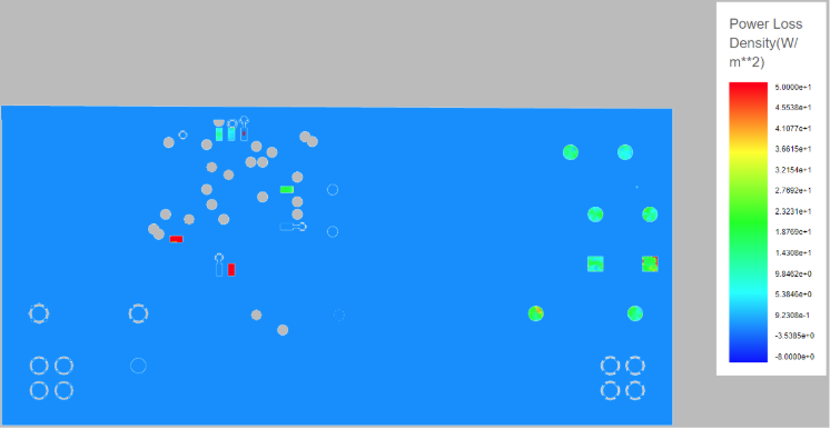
功率损耗密度分布图
Power Loss Density Distribution Map
EDA软件
EDA Tools


介绍
Introduction
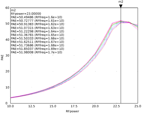
模拟射频芯片设计通常遵循一系列严格的步骤,包括规格制定、电路设计、仿真和优化、布局设计、物理验证等。芯片设计工程师需要使用专业仿真工具和器件模型,以确保设计满足性能和可靠性要求。本案例使用法动科技的EDA解决方案完成一个代表性的功率放大器设计。
Analog/RF chip design usually follows a series of rigorous steps,including specifications, circuit design, simulation and optimization,layout design, physical verification, etc. Chip design engineers need to use professional simulation tools and device models to ensure that the design meets performance and reliability requirements.Herein, a typical Ku-band power amplifier design, as a design example, is accomplished using a design flow from Faraday Dynamics, Ltd.
设计流程
Design Flow


仿真结果
Simulation Results
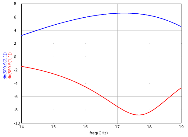
S-parameters
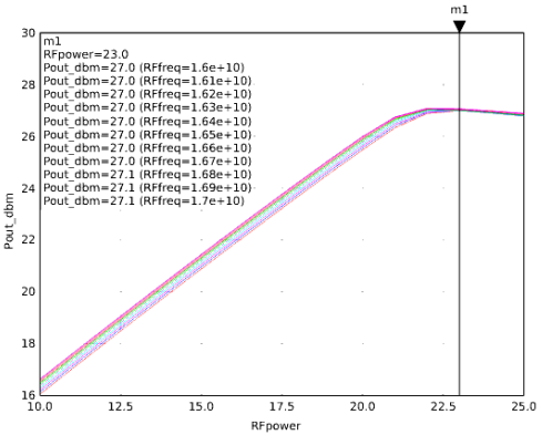
Pout
Pin
EDA软件
EDA Tools
介绍
Introduction
天线阻抗匹配是将天线的阻抗与信号源的输出阻抗或接收设备的输入阻抗协调一致,以达到信号的最佳传输状态的过程。对于发射天线而言,阻抗不匹配可能导致信号发射功率下降、发送距离减短,同时还可能损害天线组件,而对于接收天线而言,阻抗不匹配则会导致接收灵敏度降低,同时引入噪声干扰,从而影响接收信号的质量。因此,在确保良好通信性能的过程中,阻抗匹配成为至关重要的环节。
Antenna impedance matching involves aligning the impedance of the antenna with either the output impedance of the signal source or the input impedance of the receiving equipment to facilitate optimal signal transmission. Inadequate impedance matching in the transmitting antenna can result in reduced signal transmission power, shortened transmission distances, and potential damage to antenna components. Conversely, in the receiving antenna, impedance mismatch may diminish reception sensitivity and introduce noise interference, thereby compromising the quality of the received signal. Consequently, impedance matching emerges as a pivotal element in ensuring effective communication performance.

设计流程
Design Flow
仿真结果
Simulation Results
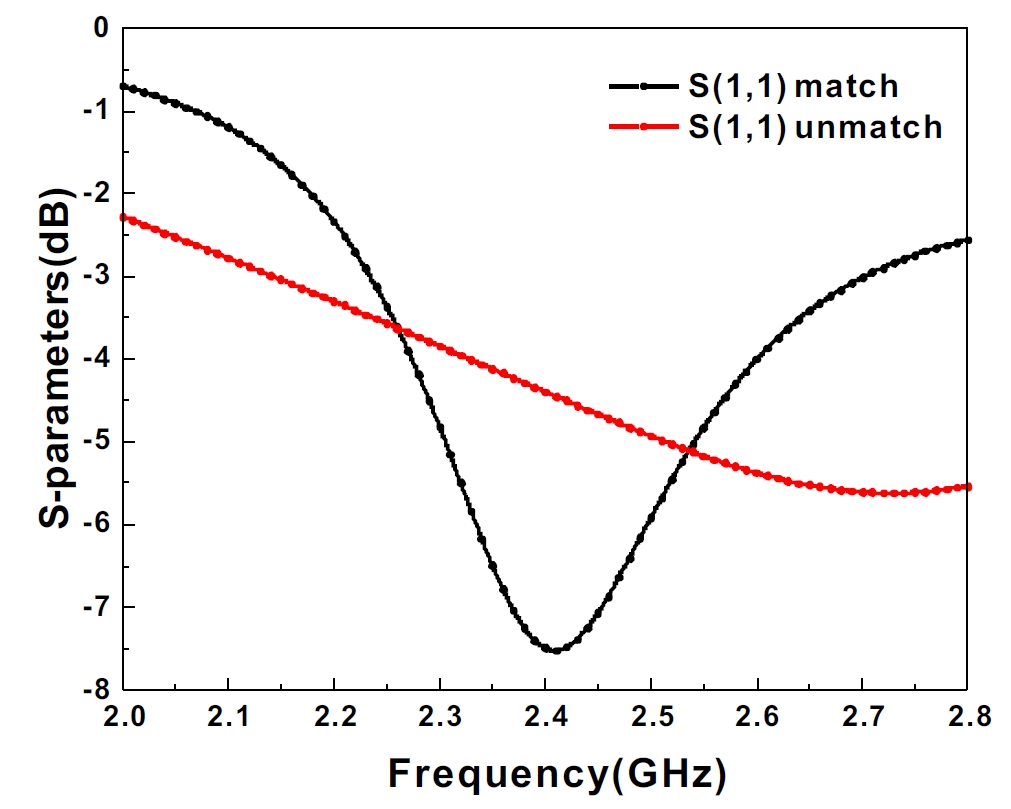
FDSPICE®将SuperEM®中仿真得到的S参数结果导入为S Model,再进行电路图搭建以及优化。可以快速得到所需R、L、C的初始值,大大降低了版图仿真的参数扫描范围,减少了整个天线匹配网络设计流程的时间。
FDSPICE® imports S-parameter acquired from simulations conducted in SuperEM® into S Model, facilitating the construction and optimization of the circuit diagram. This approach enables rapid acquisition of initial values for R, L, and C, significantly narrowing the parameter scanning range in layout simulations and reducing the overall time required for antenna matching network design.
EDA软件
EDA Tools